Quantum Dots with nanometer resolution
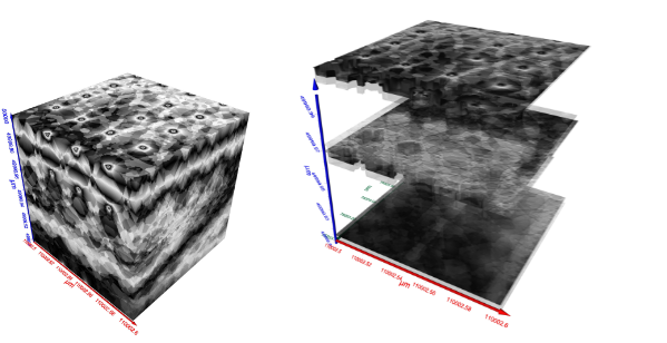
(a) 100 nm3 volume of AgI quantum dots on Si wafer (b) three different layers extracted from (a)
Chromin Salt nanoparticles – Sub-nanometer image resolution

(a) 100 nm2 area of chromim salt nanoparticles on glass slide. (b) Close up. (c) Graphical analysis of a small single grain showing <1 nm size.
Lattice stacking fault in grown semiconductors
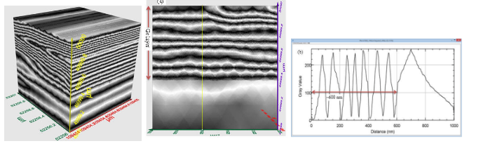
(a) Lattice stacking fault. (b) Planar image showing lattice planes and boundary. (c) Graphical analysis of dimensions.
Carbon Nanotube Film

Carbon nanotube film on Si wafer: (a) unaligned (b) 60° aligned
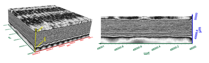
GaN on SI Wafer

(a) Three dimensional image of 1 cubic micron volume of a “GaN on Si” wafer. (b) One square micron surface image of the same (YZ plane). Distorted lattice patterns are visible indicating damages of the GaN layer.
Graphene
(a) 3D image of graphene exfoliate layers on Si wafer. (b) A single side (YZ surface) extracted from (a)
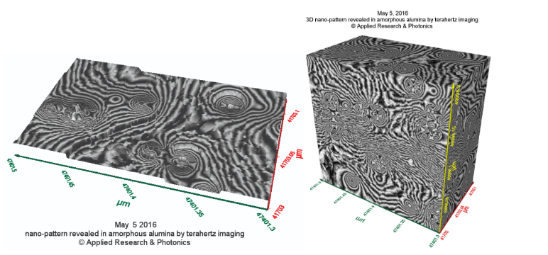
Amorphous Alumina