TeraSpectra is an innovative Terahertz Nano-Scanning Spectrometer with 3D Imaging system that breaks the spatial resolution limit of current generation optical inspection technologies, and uniquely identifies location and depth where defects exist.
 TeraSpectraA Revolutionary 3D Nano-Scale Sub-Surface Material Characterization Technology
 Key Features & BenefitsSub-Surface Layer by Layer Inspection | Sub-Nanometer Resolution | 3 Dimensional Imaging
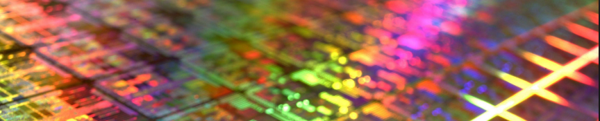
 Target MaterialsSemiconductor Wafers | Nano-materials | Soft Materials | Nano-Composites
ARP provides terahertz nano-scanning material characterization and testing services that helps semiconductor and nano-material researchers and manufacturers, easily visualize and identify using 3-dimensional images, surface and sub-layer defects.
Key Features & Benefits
• Non-Contact & Non-Destructive Testing
• Sub-Surface Layer by Layer Inspection
• Sub-Nanometer Resolution
• 3-D Imaging
• Fast Turnaround Testing
Why Applied Research & Photonics, Inc.?
Applied Research & Photonics, Inc. (ARP) provides technology and services that are revolutionizing semiconductor and nano-material research, testing and analysis. TeraSpectra, is our ground breaking and award winning Terahertz Scanning Spectrometer that provides non-contact, non-destructive, ambient temperature testing that offers two key innovations.
- it breaks the spatial resolution limit of current generation optical inspection technologies, and
- it uniquely identifies location and depth where defects exist.
Currently, there is no measurement technology that has the capability to provide an equivalent richness of information that our TeraSpectra system can deliver without damage or destruction of the test sample.